Raman Spectroscopy for Label Free ImagingResearch Stories

Prashant Jain

Nano Letters

Integrated Nanogap Platform for Sub-Volt Dielectrophoretic Trapping and
Real-Time Raman Imaging of Biological Nanoparticles

Introduction

At the University of Minnesota, the lab of Sang-Hyun Oh is working on using nanotechnology and optical methods to advance analytical and sensing method in particular for bio and life science applications. They developed a high-resolution micro Raman spectroscopy system for fast measurements (the researchers talk about a factor 100x advantage in speed over similar systems) where the biological nano particles do not have to be labelled.

The team build microscopic traps for the nanoparticles using an effect called dielectrophoresis on plasmonic nanostructures. The traps capture the bio structures along a small gap that is imaged to a spectrograph so Raman spectra of all captured particles can be collected simultaneously. In addition to this multiplexing advantage gold nanoparticles are used to create a SERS surface enhanced Raman effect to obtain even stronger signals.

for real time monitoring of bio particles in cells. Having such a system will improve capabilities for cell and biological analysis and could lead to development of more capable biosensors.

Further Information

Photothermal Conversion ProcessResearch Stories

Guowei Yang, Sun Yat-sen

Science Advances

The optical duality of tellurium nanoparticles for broadband solar energy
harvesting and efficient photothermal conversion

Introduction

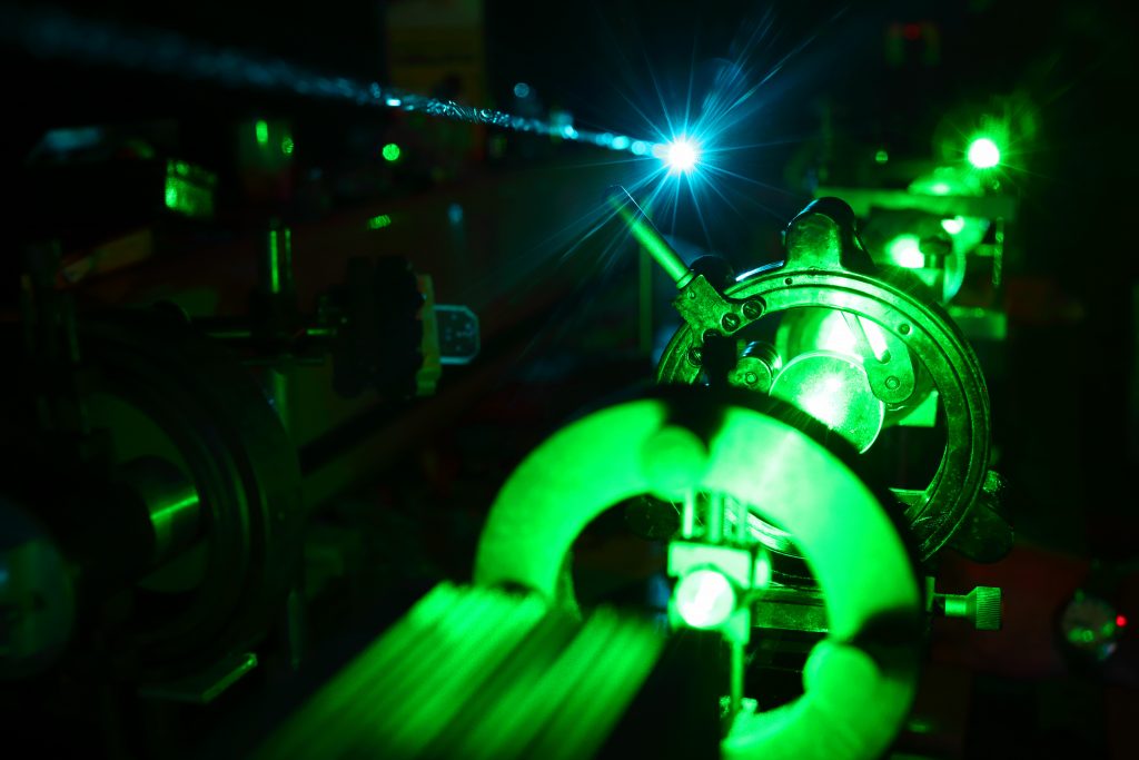
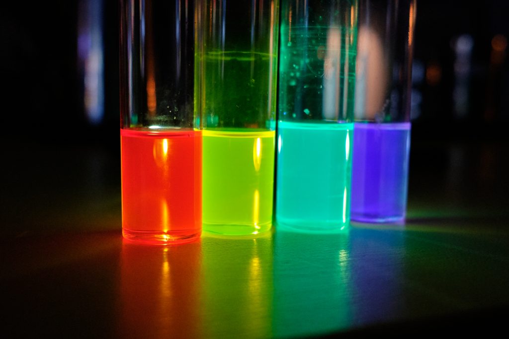
The conversion of solar energy is an area of large impact for nanotechnologies. Several spectroscopic techniques are used to probe the properties and applications of nanoparticles. Researchers from China recently published an article about Tellurium nanoparticles for conversion of solar energy. They employ Raman spectroscopy, UV-VIS absorption spectroscopy and dark field scattering spectroscopy to understand the particles properties. The research is featured on Laser Focus World with the article below:

For at least the last decade, “solar thermal” technologies, in which sunlight is used to convert water into steam that runs electric turbines or performs desalination, has been great for the investment community. About six years ago, nanoparticles started to get into the solar-thermal game when Rice University researchers added some nanoparticles to cold water and were able to make steam when they exposed the combination to sunlight.

Since then, a lot of work in what is now termed photothermal conversion has turned to the field of plasmonics, which exploits the wave of electrons that is produced when photons strike a metallic surface. However, producing plasmonic nanostructures is certainly not as straightforward as just adding some nanoparticles to water.

Now, researchers in China have combined the ease of adding nanoparticles to water with plasmonics to create a photothermal conversion process that exceeds all plasmonic or all-dielectric nanoparticles previously reported. Researchers at Sun Yat-sen University (Guangzhou, China) demonstrated in the journal Science Advances what they claim is the first material that simultaneously has both plasmonic-like and all-dielectric properties when exposed to sunlight.

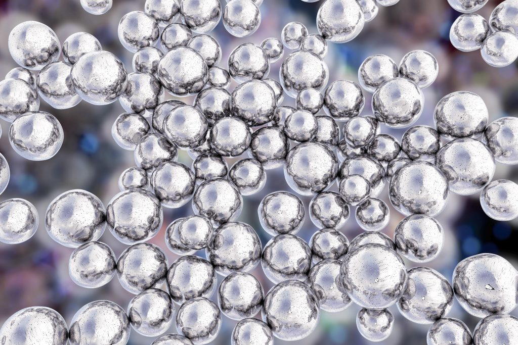
The key to achieving this combination is the use of tellurium (Te) nanoparticles, which have unique optical duality, according to G. W. Yang, professor at Sun Yat-sen University and coauthor of the research.

By dispersing these nanoparticles into water, the water evaporation rate is improved by a factor of three under solar radiation. This makes it possible to increase the water temperature from 29 degrees to 85 degrees Celsius within 100 seconds.

“The Te nanoparticles perform like a plasmonic nanoparticle when it is smaller than 120 nanometers [nm] and then as a high-index all-dielectric nanoparticle when those nanoparticles are larger than 120 nm,” said Yang. The Te nanoparticles are able to achieve this duality because they have a wide size distribution (from 10 to 300 nm). This enhanced absorption can cover the whole solar radiation spectrum.

Another property of the Te nanoparticle is that when it is excited by sunlight, the excitation energy is transferred entirely to the carriers (electrons and holes). This pushes the carriers out of equilibrium and into special states of momentum with higher temperatures.”

Yang explains that as the system evolves toward equilibrium, these carriers relax. As the carriers scatter, it leads to a phenomenon known as Coulomb thermalization, which forms a hot gas of thermalized carriers that couple with phonons and transfer their excess energy to the lattice. This results in the efficient heating of the Te nanoparticles.

For this approach to work for commercial desalination, Yang acknowledges that the current method of producing the Te nanoparticles with nanosecond laser ablation in liquid is limited. “Now, we are trying to prepare the Te nanoparticles by other methods,” he added. But because the Te nanoparticles have a unique optical duality, Yang envisions other applications for the technology. “We want to apply them in sensors or nanoantennas,” he said.

The abstract for the paper published in Science Advances details the research findings:

Nanophotonic materials for solar energy harvesting and photothermal conversion are urgently needed to alleviate the global energy crisis. We demonstrate that a broadband absorber made of tellurium (Te) nanoparticles with a wide size distribution can absorb more than 85% solar radiation in the entire spectrum. Temperature of the absorber irradiated by sunlight can increase from 29° to 85°C within 100 s. By dispersing Te nanoparticles into water, the water evaporation rate is improved by three times under solar radiation of 78.9 mW/cm2. This photothermal conversion surpasses that of plasmonic or all-dielectric nanoparticles reported before. We also establish that the unique permittivity of Te is responsible for the high performance. The real part of permittivity experiences a transition from negative to positive in the ultraviolet-visible–near-infrared region, which endows Te nanoparticles with the plasmonic-like and all-dielectric duality. The total absorption covers the entire spectrum of solar radiation due to the enhancement by both plasmonic-like and Mie-type resonances. It is the first reported material that simultaneously has plasmonic-like and all-dielectric properties in the solar radiation region. These findings suggest that the Te nanoparticle can be expected to be an advanced photothermal conversion material for solar-enabled water evaporation.

SOURCE:

IEEE; https://spectrum.ieee.org/nanoclast/semiconductors/nanotechnology/nanoparticles-take-solar-desalination-to-new-heights

Further Information

Controlling Plasmonics Using Copper NanostructuresResearch Stories

Harald Gießen

ACS

Electrochemistry on Inverse Copper Nanoantennas: Active Plasmonic
Devices with Extraordinarily Large Resonance Shift

Introduction

Prof. Harald Gießen’s group from the University of Stuttgart (Germany) is working on using photonics and nanotechnologies for new applications and devices. The researchers are looking at technologies to create displays operated by controlling plasmonic effects. Plasmonics deals with interactions of light with metallic nanostructures which can be designed to show strong reaction to light at very specific wavelength. For a dynamic, changeable display the position of these resonance wavelengths has to be controlled ideally by applying electrical voltage to the device. The researchers from Germany are creating devices based on thin Cu films with nanostructures etched into them immersed in an electrolyte solution. When applying a voltage, the Cu is electrochemically changed (oxidized or reduced) changing the color of light reflected from the device.

The setup for spectral reflectance measurements is realized using an Isoplane/PIXIS spectroscopy system. Prof. Gießens company NT&C builds microspectroscopy equipment for sensitive bright and dark field spectroscopy using Isoplane and SpectraPro HRS systems.

Further Information

Coherent Anti-Stokes Raman Scattering with
ICCD CamerasResearch Stories

Hideaki Kano

Chemistry Letters

Ultrabroadband multiplex coherent anti-Stokes Raman scattering (CARS)
microspectroscopy using a CCD camera with an InGaAs image intensifier

Introduction

Researchers from Japan show the use of ICCD cameras with InGaAs intensifier for coherent anti-Stokes Raman scattering measurements. Unlike detection with conventional CCDs an ICCD is able to restrict signal collection to a single pulse of a high repetition rate excitation system

Coupled to a high throughput, lens based spectrograph the camera makes, according to the researchers, a “powerful apparatus for obtaining CARS spectra with shot-by-shot measurement” that is able to “simultaneously detect the entire spectral region of the CARS signal in the fundamental vibrational modes”. Excitation is achieved with a 1064nm laser and broad supercontinuum pulse.

Further Information

SESORS For Deep Tissue Biological ApplicationsResearch Stories

Tuan Vo-Dinh

Advanced Biomedical and Clinical Diagnostic and
Surgical Guidance Systems XVI

Surface-enhanced patially offset Raman spectroscopy (SESORS) for
biomedical applications

Introduction

A team from Duke University in the US is using Raman spectroscopy for sensing in biological tissue. Raman spectroscopy is being used for several applications in life sciences, the researchers mention cancer detection, inflammation monitoring and measurements of glucose levels as examples.

In their article they show recent progress on measuring signal from surface enhanced Raman scattering (SERS) probes using a spatially offset Raman spectroscopy technique. The combined approach is often called SESORS and is investigated by several research groups around the world. The team from Duke show that they can isolate the SERS spectra from nanoparticles deep inside tissue.

A high throughput detection system optimized for the NIR (where tissue fluorescence is low) with wide aperture and ability to resolve several spectral channels is ideal for these measurements.

Further Information

Tomographic Measurements of PlasmasResearch Stories

Yann Camenen

Scientific Reports

Spatially resolved determination of the electronic density and temperature by a visible spectro-tomography diagnostic in a linear magnetized plasma

Introduction

Understanding and controlling the behavior of plasmas has wide applications, from surface treatment and etching in material fabrication to research in propulsion and energy production. Plasmas are states of matter and are comprised of ions and free electrons. The electron temperature and density in a plasma are two important parameters when investigating plasmas.

Although there are electronic methods which measure the electron density and temperature (using so called Langmuir Probes), optical techniques, such as scattering measurements or optical emission spectroscopy, have the advantage of not needing physical probes that could perturb the plasma.

A team of researchers in France and Germany are now showing, via a paper published in Scientific Reports, how to perform optical measurements of a plasma with both spectral and spatial resolution. Their technique is called spectrotomography and uses line of sight emission spectroscopy. For line of sight measurements an optical fiber is positioned in the focus of a small lens so that the emission along the path is detected by the lens.

The researchers combined a total of 49 fibers to study the plasma through an optical window of a vacuum chamber and detected the signal across the fibers simultaneously. An aberration corrected IsoPlane spectrograph, in combination with a large format ProEM EMCCD camera, were used for detection. A good imaging spectrograph is necessary to spectrally and spatially resolve all spectral channels at the same time. The whole instrument is spectrally calibrated to measure the correct emissivity of the plasma.

Argon emission lines are being used for tomographic reconstruction of temperature and electron density and the publication describes in detail how the results are validated using other measurement methods. The researchers conclude that their work shows the “powerful ability of the spectro-tomographic diagnostic to acquire simultaneously 2D integrated intensity of several emission lines to access a wide kind of physical parameters”. The team is working on improved methods to improve the spatial resolution using a larger number of spectral channels.

Further Information

Continuous Filter System for Detecting Raman
Scattered LightResearch Stories

Tom Vosch

Scientific Reports

Photon Energy Dependent Micro-Raman Spectroscopy with a Continuum
Laser Source

Introduction

Raman spectroscopy typically requires precise, stable and narrow band light sources to produce well defined and sharp spectral features. Therefore, emission lines from gas lasers are often used as excitation sources. However, it can be important to continuously tune the excitation wavelength. For example, some materials like carbon nanotubes, quantum dots or nanowires show resonant Raman features where the scattering intensity is strongly enhanced when exciting at exactly the right wavelength. Also, some Raman features can show energy shifts when the excitation source energy changes like the so-called D band lines in graphene materials.

While typically the energy shift in Raman scattering is roughly independent of excitation energy the D bands involve influence of defects which allows for the shift of the Raman energy.

Researchers from the lab of Tom Vosch have developed a continuous filter system based using monochromator as tunable filters and to detect the Raman scattered light. They describe how they implemented the system and synchronized movement of several system components to create a continuously tunable source using a supercontinuum laser for light input. They demonstrate the validity of their system by observing the behavior of the well understood Raman lines of graphene.

Further Information

Graphene Quantum Dots as High Purity Single
Photon SourcesResearch Stories

Jean-Sebastien Lauret

Nature Communications

Single photon emission from graphene quantum dots at room temperature

Introduction

Researchers around Jean-Sebastien Lauret from France are researching new materials like graphene and hybrid perovskites for use in quantum, plasmonics, nanophotonics and magnetometry applications. They have shown that graphene quantum dots can be used as high purity single photon sources. These special light sources are important for quantum research applications and quantum computers.

The researchers are using a microscopic photoluminescence setup for their measurements. One measurement channel determines the single photon character of the source by measuring the correlation between signal on two photodiodes.

The other channel is for sensitive, dispersive PL spectroscopy using a SpectraPro spectrograph with a Pylon camera. The PL spectrum is an important characterization tool in nanophotonics measurements. For example, the spectrum of the graphene quantum dots changes significantly when the edges of the graphene crystallites are chemically changed. Comparing the measured spectra to theoretical predictions gives the researchers confidence that they understand the size, shape and composition of their target samples.

Further Information

Making effective light absorbers from 2D materialsResearch Stories

Haiming Zhu

J. Chem. Phys

Efficient hot-electron extraction in two-dimensional semiconductor heterostructures by ultrafast resonant transfer

Introduction

Prof. Haiming Zhu and his research team at Zhejiang University in China investigate multiple aspects of 2D materials and van-der-Waals heterostructures involving their behavior when excited by light. Van-der-Waals heterostructures are layers of atomically thin 2D materials that can be stacked in specific orders to achieve desired device properties. They are studied around the world as this new class of devices can have physical properties and behavior that can’t be achieved with similar bulk structures.

Prof. Zhu’s group recently investigated the suitability of van-der-Waals heterostructures for efficient light harvesting and report on their experiments and findings in a new article in the Journal of Chemical Physics. Their findings are relevant for photovoltaics and opto-electronic devices that are traditionally bound by the 30% Shockley-Queisser limit for efficiency. However, in 2D materials this limit can be exceeded if high energetic or hot photo-excited charges can be extracted fast enough at the material interface of the device to not recombine either by light emission or nonradiative processes.

The researchers built van-der-Waals heterostructures from transition metal dichalcogenides MoTe2 and WS2, which are investigated using optical techniques, that are very common for the characterization and investigation of 2D materials. Prof. Zhu’s group uses photo-luminescence (PL) spectroscopy, absorption spectroscopy and transient pump-probe absorption spectroscopy for their experiments.

The setup for PL and absorption spectroscopy involves detection from the visible into IR wavelength covering a range from 2.1eV (590nm) to 0.9eV (1370nm) due to the broadband material characteristics. A Pylon-100 camera is used for efficient detection from visible to NIR and a Pylon-IR cryogenic InGaAs array for detection above 1000nm. For transient absorption spectroscopy a pump-probe setup is used pumping the samples with an ultrashort 35fs pulse and using a ProEM-1600 EMCCD camera for detection.

PL spectroscopy is used for the initial characterization of the materials and identifying the number of layers to find suitable samples for producing the stacked structures. By observing the behavior of the PL emission between the original and stacked layers the researchers identified changes to the electronic environment and interactions of charges when the materials are combined. For example a strong emission line of WS2 around 2eV is strongly suppressed in the stacked layer indicating the ultrafast charge transfer to MoTe2 layer. The transient absorption measurements then allows the researchers to reveal the details of the charge carrier behavior and what the mechanism for the charge transfer and its efficiency is for this particular structure.

In their conclusion the team notes that they could show effective charge transfer in the investigated structure, making these materials suitable for highly efficient devices. They note that their “findings […] enable fresh and exciting opportunities for designing extremely thin absorber and hot-carrier devices using 2D” van der Waals hetersostructures.

Further Information

Doppler Shift for Particle Beam DiagnosisResearch Stories

Arnab Deka

Journal of Applied Physics

Evaluation of beam divergence of a negative hydrogen ion beam using
Doppler shift spectroscopy diagnostics

Introduction

Fusion experiments like ITER rely on spectroscopic diagnostics to extract information from the Plasma in the reaction chamber.

Researchers worldwide are currently working on making ITER operational alongside testing subcomponents of the experiment. Here researchers from India use the doppler shift to diagnose a particle beam. They use optical fibers to probe the emission signal from different parts of their experiment and align them along the entrance slit of their spectrograph to detect the signals simultaneously on a CCD camera.

IsoPlane
PIXIS CCD Camera
SpectraPro HRS photo

Further Information