High-resolution spectroscopy for measuring fine structures and spin interactions in quantum materialsCustomer Stories

Dr. Jörg Debus

TU Dortmund University, Germany

Background

Jörg Debus and his team at TU Dortmund University in Germany conduct research on materials with high potential for applications in optical quantum information processing, spintronics as well as quantum sensing. The group studies structures, such as quantum dots, as well as 2D materials, semiconducting defects in diamond and rare-earth ions quantum wells. For optically driven spintronics and quantum information processing, the coherent spin manipulation with ultrashort laser pulses requires knowledge about the fine structures of excitons, in particular, the electron and hole g-factors: they define the frequency of quantum bits. In addition to the spin level structures, the interactions between confined carriers play a crucial role, since they limit the quantum information handling due to spin relaxation.

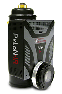
One example of experiments performed by the Debus team are recent measurements on the energy and spin structure of nitrogen vacancies in diamond crystals. Due to their unique electron confinement, the electron spins demonstrate robust coherence times exceeding several seconds at room temperature that are suitable for quantum information and quantum sensing applications. For such use it is important to know the fine structure of energy levels corresponding to different spin states in magnetic fields and understand the interaction mechanisms of charge carriers in the material. The Debus team uses optical spectroscopy to measure these properties and to spectrally resolve the fine structures.

In addition to photoluminescence spectroscopy, another technique used by the Debus team is spin-flip Raman scattering, a process similar to ordinary Raman scattering, however instead of a different phonon state the initial and final material states have different spin properties. The spin-flip signal is detected at a position that is spectrally shifted from the excitation laser line by the energy difference of the spin states. Spin-flip Raman scattering as a resonant process is not only useful for measuring spin levels, but also to prepare carriers confined in quantum dots in specific spin states. Above all, the scattering mechanism helps to identify the spin interaction between electrons and holes. Most experiments in the lab are performed at cryogenic temperatures in magnetic fields, while precisely controlling the energy and polarization of the excitation light.

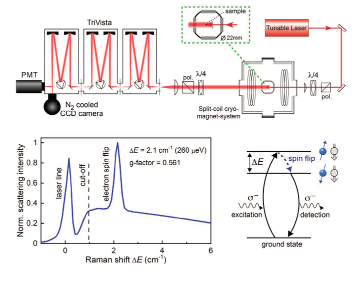
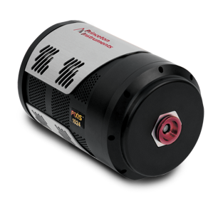
Figure 1: Top: Scheme of the TriVista setup used for spin-flip Raman scattering. Bottom, left: Raman spectrum shows the spin-flip signal of electrons confined in InGaAs/GaAs quantum dots taken at a magnetic field of 8 T and a temperature of 6 K. The excitation was done at 1.39 eV (892 nm), the detection was provided by a LN2-cooled Spec-10 CCD camera. Bottom right: Scheme of the electron spin flip (blue colored) for resonant σ- circular-polarized excitation of an exciton in oblique magnetic field geometry.

Challenge

Research in the Debus lab does not only focus on one, but on a broad range of materials. The spectroscopy system needs to adapt to changing signal wavelength and use of lasers at different excitation wavelength or tunable lasers as well as obtain sufficiently high spectral power to resolve the details of the fine structure and interactions of spin states which are tuned by an applied magnetic field.

One problem in resolving the fine structure of, for example, semiconductor quantum dots is inhomogeneous broadening due to a distribution of energy levels caused by small variations in size and shape of the quantum dots. By tuning the excitation wavelength in resonance with specific quantum dot states, the signal of other dots in the sample is suppressed reducing spectral broadening. However, laser excitation will be in close spectral vicinity of the detection signal. The same is true for signals in resonant spin-flip Raman scattering which are slightly shifted by a fraction of an meV (a few cm-1) from the excitation laser line.

Spectroscopic measurements in close vicinity to the laser line are extremely challenging. The intensity of elastic scattered light is often much stronger than the signal and interfere with the detection of weak signals on the detector. Filters have to be used to reduce the amount of laser light before detection. The filters need sharp cutoffs and transitions width to measure close to the laser line, however changing excitation wavelength typically requires use or purchase of additional filters.

The TriVista allows us to perform challenging optical spectroscopy with high resolution as close as a few 100 μeV (0.8 cm-1) from the excitation laser line

Solution

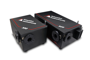
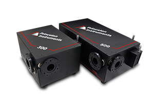
The Debus team uses a TriVista TR555 triple stage spectroscopy system to achieve not only high resolution and strong stray-light suppression (for signals close to the laser line), but also flexibility to adapt to the changing experimental requirements such as different materials, excitation and detection wavelengths. Moreover, the intensity of the spin-flip Raman scattering signals is quite low so that a high efficiency of the optical components and detector sensitivity are necessary.

TriVista systems are built from 3 spectrometer stages. By combining the diffractive power of all 3 stages high spectral resolution is achieved up to 300% higher compared to a single stage. Another operating mode combining all 3 stages allows for recording signals in the vicinity of the laser line as close as 5 cm-1 (0.62 meV) using a CCD camera for detection. In this mode of operation, the first 2 stages are linked together in a way to act as a signal bandpass filter that is spectrally dispersed by the third stage. Alternatively, the Debus team sometimes uses the high- resolution mode with a single channel detector (e.g. PMT) for detection. It also achieves high stray-light rejection and is suitable for measurements that do not require the spectral multiplexing advantage of detection using a CCD.

The TriVista system easily adapts to the changing experimental requirements of the lab. TriVista can be quickly adapted to any laser or signal wavelength from the UV to the IR without use of additional edge or notch filters that need to be changed for each operating wavelength.

TriVista systems also operate up to 4 signal output ports (one on stage 1 and stage 2, two on stage 3) and additionally to the combined operation modes described above, each stage can be operated independently of each other. The Debus team uses efficient detectors for visible and IR detection on different output ports as well as intensified CCD cameras such as the PI-MAXfor time-resolved measurements with nanosecond resolution.

Having the capability of high resolution, high stray-light reduction measurements at any wavelength as well as multiple efficient detection and operation options allows the TriVista systems to fulfil the multiple needs and requirements for all aspects of new and quantum material research by the Debus team.

Singlet Oxygen Emission to Monitor Tumor
ApoptosisResearch Stories

Brian Pogue, Scott Davis

SPIE Digital Library

A 2D imaging dosimeter for photodynamic therapy, Optical Methods for
Tumor Treatment and Detection: Mechanisms and Techniques in
Photodynamic Therapy XXVIII, 2019

Introduction

Researchers around Brian Pogue and Scott Davis from Dartmouth College in the US have published a conference report about their experiments on using 2D imaging for singlet oxygen imaging and dosimetry in cancer treatment by radiation therapy. Specifically, they perform photodynamic therapy where the photosensitizer molecule used triggers a destructive chain reaction in tumor cells on radiation. As singlet oxygen (an excited form of the oxygen molecule) is closely involved in this reaction, direct detection of emission from this molecule can be helpful in monitoring the reaction dose as well as estimating the deposited energy dose during treatments.

Highly sensitive, deeply cooled 2D InGaAs cameras are very well suited to monitor the emission of singlet oxygen. In the current study the researchers have developed several setups and they included a Princeton Instruments NIRvana to further increase the detection sensitivity. They performed extensive tests to show that the setup is very suitable for sensitive dosimetry and will continue with extensive in vivo and animal studies. This research should be extremely relevant for all researchers working in bioimaging as well as cancer research and treatment.

Further Information

Rare Earth Metals for NIR-II Bioimaging Fluorescent ProbesResearch Stories

Hongrong Liu

Materials Science and Engineering

808 nm laser-triggered NIR-II emissive rare-earth nanoprobes for small tumor detection and blood vessel imaging

Introduction

Bioimaging in the NIR-II/SWIR wavelength range is currently used to research cancer detection and treatment, monitoring metabolic and organ functions or measuring blood flow and heartrate non-invasively. The research is currently progressing from early proof of concept stages to describe more specific bio experiments using the imaging as a tool to monitor the systems. However, research to find more suitable and functional nanoprobes, small molecules and particles that emit fluorescent light in the SWIR, with the potential to be functionalized and used in vivo, is still a very important part of this research.

A research team from China is reporting on experiments using particles based on rare earth metals and they can show high performance and tunability of these probes. The functionality is shown by sensitive in vivo measurements of tumors and blood vessels. The researchers note that these probes are promising due to their bright emission as well as biocompatibility.

Further Information

Low Toxicity NIR II/SWIR Fluorescent ProbesResearch Stories

Fan Zhang

Nature Communications

Anti-quenching NIR-II molecular fluorophores for in vivo high-contrast imaging and pH sensing

Introduction

Development and testing of new molecular/nano-bio probes is an important part of NIR-II/SWIR biological imaging and diagnostics. Research in particular is focused on finding probes of high efficiency that can be used in human/clinical applications. Previously the lab of Moungi Bawendi at MIT successfully demonstrated use of a fluorophore called indocyanine green (ICG) which is clinically approved but does not optimally emit radiation in the desired wavelength range

In a recent article in Nature Communications researchers around Fan Zhang from Fudan University (Shanghai, China) developed molecules similar to ICG but optimized to emit in the NIR-II/SWIR wavelength range while still exhibiting low toxicity for potential clinical applications. The researchers demonstrate imaging up to 8mm into tissue as well as reliable, non-invasive measurements of pH values in mouse stomachs. Having demonstrated the basic use of this class of fluorophores opens up the path to more wider applications in biomedical sensing.

Further Information

NIR Detection of SWCNTs for In Vivo StudiesResearch Stories

Tara Sabo-Attwood

NanoImpact

Utilization of near infrared fluorescence imaging to track and quantify the pulmonary retention of single-walled carbon nanotube in mice

Introduction

Several analytical methods have been commonly employed for carbon nanomaterial detection including electron microscopy (TEM/SEM), Raman spectroscopy, and mass spectrometry. However, each has limitations, for example a lack of spatial resolution specificity for differentiating carbon nanomaterials from the carbon in the biomass of living organisms. Near IR fluorescence imaging has emerged as promising tool for detection and quantification of singlewalled carbon nanotubes (SWCNTs) for in vivo studies.

Collaborating researchers from the University of Florida, University of Texas and Duke University in the US published a study demonstrating that near infrared fluorescence was an effective method for pulmonary retention of SWCNTs in a murine model. They used a custom imaging system based on detection with a Princeton Instruments OMA V, 2D InGaAs array for capturing the emission from carbon nanotubes. The concentration of nanotubes is deliberately chosen to be at or below the detection threshold of other technologies such as Raman spectroscopy. The experiments use pristine, unaltered and not functionalized nanotubes. The methods are also applied on tracking and quantifying concentration of carbon nanotubes in lung tissues to assess pulmonary retention and distribution leading to potential health effects in mice.

Further Information

NIR Spectrometry for Characterizing Laser EmissionsResearch Stories

Marcin Syperek

arXiv

Observation of gain-pinned spatial dissipative solitons in a microcavity laser

Introduction

Researchers in Poland, together with collaborators in Germany, Australia and Singapore, used a NIRvana camera alongside a SpectraPro HRS spectrometer to characterize laser emissions

The researchers investigated solitons in a laser. Solitons are special, self-reinforcing waves and have important applications in building new kinds of optoelectronic devices. The emission of the devices in the IR is characterized by spectroscopy and momentum space spectroscopy while imaging of the devices is performed in 0th order of the spectrograph. Using the 2nd port of the SpectraPro HRS system a streak camera is used for time dependent spectroscopy as well.

Further Information

Characterizing Photonic Integrated CircuitsResearch Stories

C. Martin de Sterke

University of Sydney, Nature Communications

Modular nonlinear hybrid plasmonic circuit

Introduction

Si photonics is a key technology and heavily researched area due to its broad applications from quantum computing to bio sensing. Testing and characterization of photonic structures requires sensitive, precise and quantitative imaging and spectroscopy solutions from visible to infrared wavelengths (Telecom wavelength).

Photonic integrated circuits are chip scale devices that perform complex optical functions and processes using light. As optical miniaturization and devices get more complex it can be practical to follow more modular design approaches for a combination of elements with different optical functions and research. As devices get more complex, design approaches with modular character are advantageous. Such devices also have to use design strategies that combines Si waveguides with plasmonic, metallic elements that are used to achieve optical functionality on PIC platforms, with high coupling efficiency.


Researchers around Prof. Martijn de Sterke from the University of Sydney (Australia) wrote in a recent article that so called “hybrid plasmonic waveguides containing a low-index buffer layer between the metal and the high-index waveguide” provide “a convenient interface for coupling between photonic and plasmonic waveguides.” Together with collaborators from Jena and Braunschweig (Germany) the researchers around Prof. de Sterke report on their efforts to build more complex circuits of these hybrid structures, using “multiple modular, function elements”.

The researchers created a plasmonic device that rotates the polarization of an incoming TE polarized, IR beam into a TM polarized beam that is converted into a visible output through non-linear, second harmonic generation. The device incorporates nanofocusing elements, which are sharp metallic tips that confine light to a ultra-small (nanometer sized volume) leading to giant electric field enhancements and thus more second harmonic light generation.


The processed, nano-structured devices are evaluated using microscopic imaging and spectroscopy. The microscope is coupled to a spectrograph operated with 2 cameras for detection. As the devices were designed for an input wavelength of 1320nm with SHG output at 660nm, the setup used a Teledyne Princeton Instruments NIRvana camera for SWIR light and PIXIS CCD camera for visible light detection and spectroscopy. The setup performs several measurement functions:
• Imaging monitors light scattering from the nanostructures on the devices, confirming the efficiency of polarization rotation and second harmonic generation with changing design dimensions.
• Spectroscopy characterizes the spectral response, for example comparison of the input light and output light spectrum confirms the SHG nature of the visible light.
• The SHG light is measured quantitatively to obtain the spectral conversion efficiency achieved.

The article shows how nanofocusing is achieved, as the SHG sharply increases for smaller metallic tips, and they discuss how the device efficiency could be further improved. According to this research the modular design approach can be practically applied to more complex devices and is compatible with CMOS processing techniques using Cu and Al as metals without degradation of device quality. The potential applications include “on-chip quantum photonics and spectroscopy, nonlinear and atomic scale sensing, and nanoscale THz sources and detectors”.

Further Information

NIR Optical Imaging System for Deep-Tissue ImagingResearch Stories

Angela Belcher

Scientific Reports

Deep-tissue optical imaging of near cellular-sized features

Introduction

Researchers from MIT, in collaboration with Koch Institute for Integrative Cancer Research, published a breakthrough scientific report in biomedical engineering. They designed & developed an NIR optical imaging system named DOLPHIN, which stands for “Detection of Optically Luminescent Probes using Hyperspectral and diffuse Imaging in Near-infrared.” Their system holds promise for high-resolution, deep-tissue imaging. DOLPHIN achieves the following:

  • • Resolution of probes through up to 8 cm of tissue phantom
  • • Identification of spectral and scattering signatures of tissues without a priori knowledge of background or autofluorescence;
  • • 3D reconstruction of live whole animals.

For hyperspectral imaging (HSI) mode, they utilize a liquid nitrogen cooled InGaAs camera (OMA:V 2D, 256 × 320 pixel array used without binning, detection range: 900-1,700 nm, temperature –100 °C) at the exit slit of monochromator equipped with a 150 g/mm NIR diffraction gratings. To the best of their knowledge, DOLPHIN is the first demonstration of utilizing both HSI and HDI modes in a trans-illumination configuration to investigate NIR-II fluorescent signals. In contrast, previous HSI and HDI technologies worked mainly in the visible and NIR-I wavelengths, utilized either epiillumination or reflectance configurations that result in shallower depths of detection, and also relied on mapping to reference spectra to identify features of interest.

Further Information

One-Pot Synthesis of NIR-II Emissive Quantum DotsResearch Stories

Wei Huang

Inorganic Chemistry Communications

Facile one-pot synthesis of monodispersed NIR-II emissive silver sulfide quantum dots

Introduction

Fluorescence imaging in the NIR-II/SWIR wavelength range is extremely useful for locating tumors, monitoring physiological processes and studying biochemistry in vivo and non-invasively. As there is a diverse range of applications for this imaging technique, it will be useful to have different kinds of fluorescent nano agents available for targeting different types of tissue or biomolecules, for example. Ideally these agents should be very efficient in converting excitation light into fluorescent light of a small wavelength window where absorption and scattering in tissue are minimal, as well as bio-compatible and non-toxic.

Researchers around Wei Huang from Nanjing in China are reporting on quantum dots based on silver atoms and demonstrate their potential for in vivo imaging using a NIRvana InGaAs camera. While imaging is one technique necessary to demonstrate the effectiveness of a nano-particles other measurement techniques are always useful for characterization of nano-particle development. Sensitive fluorescence and/or fluorescent emission spectroscopy (for example based on single or multistage monochromators, high powered light sources and sensitive CCD detectors) can play an important role here as well.

Further Information

Advanced CMOS Detectors: Enabling the Future of Astronomical Observation

Watch our recent webinar

CMOS designs feature a combination of high QE, high dynamic range, short readout times and low noise making them a competitive alternative for a wide range of astronomy applications. If you would like to find out more about our future CMOS capabilities within astronomy, watch our on demand webinar Enabling the Next Generation of Astronomy.

Introduction

Ground based astronomy provides an accessible way to image objects in space. As most of the objects in space can be observed within the visible wavelength range (380-700 nm), optical astronomy has been at the forefront of astronomical observation. Many objects in space are very faint, requiring a camera with high sensitivity and minimal noise to detect their weak signal.

For decades, back-illuminated CCDs, with >95% quantum efficiency (QE) in the visible, have been the go-to detector choice for astronomical observation. The faint signal of objects within space often requires long exposure times to ensure detection. Figure 1 shows two images, one of the Pleiades and the other of the Milky Way taken by CCD cameras.

Figure 1: Images of A) the Pleiades and B) gravity waves and the Milky Way taken using a CCD camera. Images courtesy of Rozhen National Astronomical Observatory and Korea Polar Research Group respectively.

The ability to detect this signal is constrained by various noise sources, and this limitation is typically defined by the signal to noise ratio, or SNR.  Typically, the higher the SNR, the better the image.  There are several noise sources, including shot noise from the source and background noise from the sky, which are inherent to ground based observation [1]. 

Two additional noise sources are native to the camera, read out noise and thermal noise.  Read noise is essentially the “noise floor” of the image and is reduced by proper electronic design.  Thermal noise, or dark current, is the noise generated from thermal sources and is directly correlated to temperature and exposure.  Dark current increases with long exposures (minutes and longer) regardless of camera technology. To significantly reduce dark current, and improve SNR, back-illuminated CCDs are deeply cooled to reduce the amount of thermal noise contributing to the signal [2].  For these reasons, when very long exposures are needed to capture faint signals, CCD cameras have been the best option.

There are other applications in ground-based astronomy for which CCD’s are not the best solution.   One of these is the requirement to operate imaging sensors at faster time scales. Applications, such as time domain astronomy and space debris tracking, require faster times scales to capture as much information about dynamic objects or events.

Faster time scales are determined by the combination of exposure and readout speed. For CCD’s photons are converted into photoelectrons, and during readout, the detected photoelectrons need to be shifted to one (or sometimes a few) readout nodes, causing a bottleneck that slows readout. Fast readout on CCDs requires very fast measurement of signals at these readout nodes, performed by analog-to-digital convertors (ADCs). This high-speed measurement reduces signal quality through introducing a high level of read noise [3]. Detectors with large sensor areas and high number of pixels (4k x 4k or greater) have long readout times where no signal can be acquired, ranging from seconds to tens of seconds even at higher ADC rates.

Full frame CCDs, typically used within astronomy, require mechanical shutters to completely block any incident light during readout [4]. Mechanical shutters have finite lifetimes and often need to be replaced frequently when the camera is in heavy use. This can be problematic for observatories in remote locations where maintenance can be challenging. Additionally, opening and closing a mechanical shutter is relatively slow, leading to slower frame rates and quantitative errors for shorter exposure times.

EMCCDs, an alternative sensor technology, are typically used for more challenging, dynamic observations. EMCCDs use on chip amplification to elevate the signal relative to the read noise. With this low or negligible effective read noise, EMCCDs can operate at much higher frame rates more suitable to capture the evolution of dynamic events while maintaining the required SNR. Figure 2 shows a schematic of EMCCD sensor architecture, showing how the on chip amplification elevates the signal above read noise.

Figure 2: Schematic showing an EMCCD sensor. Photons are collected and converted into photoelectrons within the image capture area which are then transferred to the storage area. These electrons are then amplified in the extended multiplication register which increases the signal produced without increasing any read noise.

Many EMCCDs have a fast, electronic shutter where exposure is stopped by shifting detected photoelectrons into a frame storage area before readout. The electronic shutter is not only more precise than mechanical shutters, but also leads to lower dead time of the detector during which the camera is not exposing to light, as subsequent exposures can already start as signal is readout from the storage area. This is referred to as ‘High duty cycle’.

Although EMCCDs can operate at higher frame rates, duty cycles and are ideal for the detection of ultra-weak signals, they are limited by excess noise. This additional noise source is caused by the random nature of the on-chip amplification process and causes a sacrifice in overall sensitivity for signals larger than a few photons per pixel. For more information on these limitations, please refer to our article Types of Camera Sensor [5].

The Advantages of Advanced CMOS Technology

Traditional CMOS sensors have not been widely considered for astronomical observation as they are front illuminated, typically having low QE and operating at higher read noise and poorer linearity (proportionality between detected signal and digital signal) compared to CCD and EMCCD sensors. However, advancements in CMOS technology now allow CMOS to not only match these parameters of CCD and EMCCD sensors, but to also overcome the common limitations of these technologies.

Back-Illuminated CMOS Technology

The introduction of back-illuminated CMOS sensors has significantly increased QE, achieving >90% for visible wavelengths.  In addition, advanced CMOS sensor design, such as Teledyne Imaging’s LACera™ technology, shows increased sensitivity in the UV with respect to a typical CCD (see Figure 3). This makes advanced CMOS detectors not only ideal for observations in the visible wavelength range, but also for those which utilize the UV spectrum.

Figure 3: Quantum efficiency curve of an advanced CMOS sensor and a typical back-illuminated CCD sensor.

CMOS Sensor Architecture

Unlike CCD sensors, the charge to voltage conversion on CMOS sensors takes place in every pixel individually (see Figure 4), with the readout nodes on every column of the sensor operating simultaneously. This parallel readout architecture provides a tremendous speed advantage, allowing CMOS sensors to process acquired data at a much faster rate while achieving lower read noise than CCDs, and without the excess noise of EMCCDs.

Fast readout is not only important for dynamic astronomical imaging, but also for quick decision making and analysis such as in adaptive optics systems for correction of atmospheric turbulence. CMOS sensors also use precise electronic shutters allowing for continuous imaging without loss of data. 

Figure 4: Schematic showing a full frame CCD readout architecture in comparison to a CMOS readout architecture. Pixels on the full frame CCD are shifted vertically down the sensor until they read the readout array. They then shift horizontally, pixel-by-pixel, until they are read out by an Analog-to-Digital Converter (ADC). In comparison, CMOS architecture has an individual ADC per column, increasing the speed of readout while maintaining a low read noise.

High Dynamic Range

Within astronomy, it is not uncommon to have both bright and faint objects within the same field of view. High dynamic range (HDR) makes the detection of faint astronomical objects possible without saturating the detector with light from surrounding brighter objects. HDR operation depends on linearity, ADC bit-depth and gain. CMOS cameras can extend dynamic range through multiple sampling of the signal with high and low gain. However, artifacts in the cross-over between high and low gain readouts can limit measurement precision.

Advanced CMOS designs, such as Teledyne Imaging LACera™ technology, ensure precise cross-over between both ADCs for operation with low noise and high linearity. Combined with higher bit-depth ADCs, LACeraTM technology provides unsurpassed dynamic range. More details about HDR operation of LACeraTM technology can be found in our article New Era in High Dynamic Range CMOS [6].

True Global Shutter

CMOS sensors typically begin exposure, read out and clear the sensor row-by-row, via a process called a rolling shutter. Although this process is very fast, it can introduce distortions to fast-moving objects, potential delays between frames, and difficulties with synchronization which would be detrimental for many astronomy applications (see Figure 5).

Figure 5: The camera sensor is shown on the left, with rolling shutter architecture meaning that exposure does not begin for the entire sensor at the same time, but exposure and readout move from the top to the bottom of the sensor. The time dimension is shown from left to right, with which rows are reading out indicated on the vertical axis. The timescale of the rolling behaviour is the camera’s Frame Time, typically around 20ms.

Alternatively, global shutter, which reads and resets all detector pixels simultaneously, is challenging to engineer for back-illuminated CMOS sensors. For global shutter devices, to end an exposure, photoelectrons need to be moved immediately into a storage area. This storage area is typically light-sensitive, meaning that artifacts can arise from unwanted photons interacting with it.

The storage area can be hidden under sensor components for front-illuminated CMOS sensors; however, this is more challenging with back-illuminated technology. Advanced back-illuminated CMOS technology, like that of LACera technology, redesigns the storage area to achieve true global shutter operation without artifacts. Find out more about this process in our article: Achieving a True Global Shutter with Large Format, Back-Illuminated CMOS [7].  

Large Field of View

Parallelization and high-speed operation make CMOS designs ideal for large area sensor designs. CMOS cameras have now been developed with pixel counts of 6k x 6k and above, alongside large pixel sizes (10 μm) featuring high QE and low read noise required for precise imaging of fainter, high speed objects, or multiple fainter objects within one frame.

Benefits of large sensor sizes include fewer telescope movements for tracking rapidly moving objects (space debris), observing more objects per frame (sky surveys) and better image calibration by observing more reference stars.

Summary

Although CCD and EMCCD technologies have their advantages within ground based astronomical imaging, back-illuminated CMOS camera technology matches their specifications while overcoming their limitations on speed, duty cycle and noise performance.

CMOS designs feature a combination of high QE, high dynamic range, short readout times and low noise making them a competitive alternative for a wide range of astronomy applications. If you would like to find out more about our future CMOS capabilities within astronomy, sign up to our webinar Enabling the Next Generation of Astronomy.

References

[1] Signal, Noise and Detection, O.Hainaut, 2005-Jun-01, URL: http://www.sc.eso.org/~ohainaut/ccd/sn.html

[2] Dark Current, Teledyne Photometrics, accessed 11/01/2021 https://www.photometrics.com/learn/imaging-topics/dark-current

[3] Readout vs. Frame Rate, Teledyne Photometrics, accessed 11/01/2021 https://www.photometrics.com/learn/imaging-topics/readout-vs-frame-rate

 [4] G. Kasprowicz et al., CCD detectors for wide field optical astronomy, Photonics Letters of Poland, 1 (2), 2009

[5] Types of Camera Sensor, Teledyne Photometrics, accessed 11/01/2021 https://www.photometrics.com/learn/white-papers/types-of-camera-sensor

[6] New Era in Dynamic Range and Linearity for Scientific CMOS Cameras, Teledyne Princeton Instruments, https://www.princetoninstruments.com/products/technologies-family/lacera/tech-notes/new-era-in-dynamic-range-and-linearity-for-scientific-cmos

[7] Achieving a true global shutter with large format, back-illuminated CMOS, Teledyne Princeton Instruments, https://www.princetoninstruments.com/products/technologies-family/lacera/tech-notes/achieving-a-true-global-shutter-with-large-format-back-illuminated-cmos

Further Reading

COSMOS for Time Domain Astronomy

Find out how COSMOS provides large format, low noise, and high quantum efficiency essential for time domain astronomy.

Advanced CMOS for Dynamic, Faint Astronomy

Find out how advanced CMOS provides an alternative to EMCCDs for dynamic, faint astronomy when there are more than a few photons signal.

New Era in Dynamic Range and Linearity

Find out more about how innovations in the CMOS readout process now offers unsurpassed dynamic range and linearity.