Two dimensional materials, i.e. materials that can be produced in crystalline, single atomic layers, have opened up a wide field of research investigating the physics and engineering of these structures. For engineering new devices, scientist build so called van-der-Waals heterostructures where they combine different 2D materials in layered stacks and probe them by electrical and optical methods. Combining different materials can significantly change the physical properties of the materials itself
Researchers from Japan report on experiments with materials encapsulated in hexagonal Boron-Nitride (hBN), i.e. they are completely enclosed in an hBN layer to their bottom and top sides. While this is typically done to preserve the pristine properties of the 2D materials, their optical measurements show that hBN itself alters the physical properties of the encapsulated material.
The experiments use sensitive temperature dependent microspectroscopy to monitor the PL emission. The setup to measure the weak PL signal is realized using an Isoplane spectrograph. For tunable excitation the researchers use a supercontinuum laser source coupled to a SP-2150 monochromator.
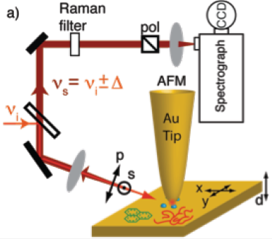
Researchers around Prof. Yousoo Kim from the Surface & Interface Science Laboratory at RIKEN in Japan use tip enhanced Raman spectroscopy (TERS) or more specifically scanning tunnelling microscopy TERS to investigate single molecules on very thin insulating films. The team shows in a recent study that the resolution of their setup is so high that they are able to resolve the shape of individual vibrational modes with submolecular resolution. The researchers think that their experimental approach will be useful for the discovery of new materials and their properties.
The researchers are observing single copper naphthalocyanine (CuNc) molecules on Ag crystals. The molecules are placed on an ultrathin, triple-layer insulating NaCl to prevent them from interacting with the Ag surface, so the intrinsic properties of the CuNc molecules can be observed.
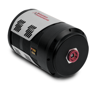
For TERS an atomically fine tip is brought in very close contact to the molecule. Strong electric field enhancement due to the tip leads to a magnification of the Raman signal of the molecule. TERS measurements are extremely challenging,in particular on the single molecule level, due to the inherently weak Raman signals and very sharp Raman peaks. For achieving high signal to noise the experiment setup uses an Isoplane 320 system and PIXIS camera.
Transition Metal Dichalcogenides are semiconductor materials that build single atom thin layers. They are heavily researched with other materials as two dimensional materials and have been discovered to be useful materials for nanophotonic applications either on their own or combined in stacks with other 2D materials (so called van-derWaals heterostructures). Many experiments investigate their behavior in combination with plasmonic and cavity nanostructures. Such devices allow investigation of interesting physics and are building blocks for components of photonic and quantum devices.
A new publication by a research collaboration around Prof. Tian Jiang and Prof. Lei Shi in China is reporting on their experiments combining monolayers of Tungsten diselenide with photonic crystal structures. Such nanostructures have a strong influence of the energy as well as direction of light emission. Energy-momentum spectroscopy is a perfect tool to observe the properties of these devices. This technique is equivalent to Fourier plane imaging in microscopy where instead of the direct image of the sample, the back-focal plane of the objective is observed, which reveals the direction of light emission. If this image is projected on the entrance slit plane of a spectrograph the relationship between light wavelength and its momentum can be directly observed.
In the reported experiment the energy-momentum spectroscopy system is built around an Isoplane-320 spectrograph combined with a PIXIS 400 camera. Aberration corrected systems are perfectly suited for these measurements as important information is observed across the whole image sensor. The researchers report that their energy momentum measuremetns reveal strong coupling in their device which allows them to study fundamental physics as well as show the potential of this material for applications in nanophotonic devices in the future.
Researchers around Fan Zhang demonstrate a new molecule for in-vivo imaging where both excitation and emission of the molecule are optimally in the SWIR/NIR-II spectral range.
They show high resolution imaging of brain tissue as well as dynamic imaging of the respiratory rate of mice by imaging movements of the liver.
Researchers around Jianhua Hao demonstrate targeted in vivo imaging with a new emission probe. The fluorescent molecule has a bright and relatively small band emission around 1330nm and is rapidly excreted by a life organism making it very suitable for clinical NIR-II imaging applications.
The researchers show imaging of kidney function and filling of a mouse bladder as well as detection of small millimeter sized tumors. Furthermore, the researchers can combine their technique with X-ray imaging as the probe is a good X-ray imaging agent as well.
Confocal microscopes are widely used in physical and in particular life sciences as they offer higher resolution as standard widefield imaging. If high acquisition speeds and frame rates need to be achieved typically scanning confocal systems are used that permit to scan a field of view with an excitation light source with kHz rates
The research group of Ardemis Boghossian from Lausanne, Switzerland has just published a report about their research in collaboration with Nikon and Crest Optics to transfer scanning disc confocal microscopy to the SWIR/NIR-II wavelength range using a Princeton Instruments NIRvana-ST camera for detection.
SWIR imaging is increasingly established in life science due to low absorption and scattering of tissue in this wavelength band. The researchers show with several application examples that the new setup increases the spatial resolution while still allowing for image acquisition at high frame rates. For example, carbon nanotubes can be precisely localized in chloroplasts, monitoring nanoparticle movement in solvents allows to measure diffusivities and using the high vertical resolution allows for glucose concentration measurements using nanosensors at different depth of a sample. This research lays the groundwork for establishing and expanding this technique to monitor the location and movement of nanoparticles and sensors.
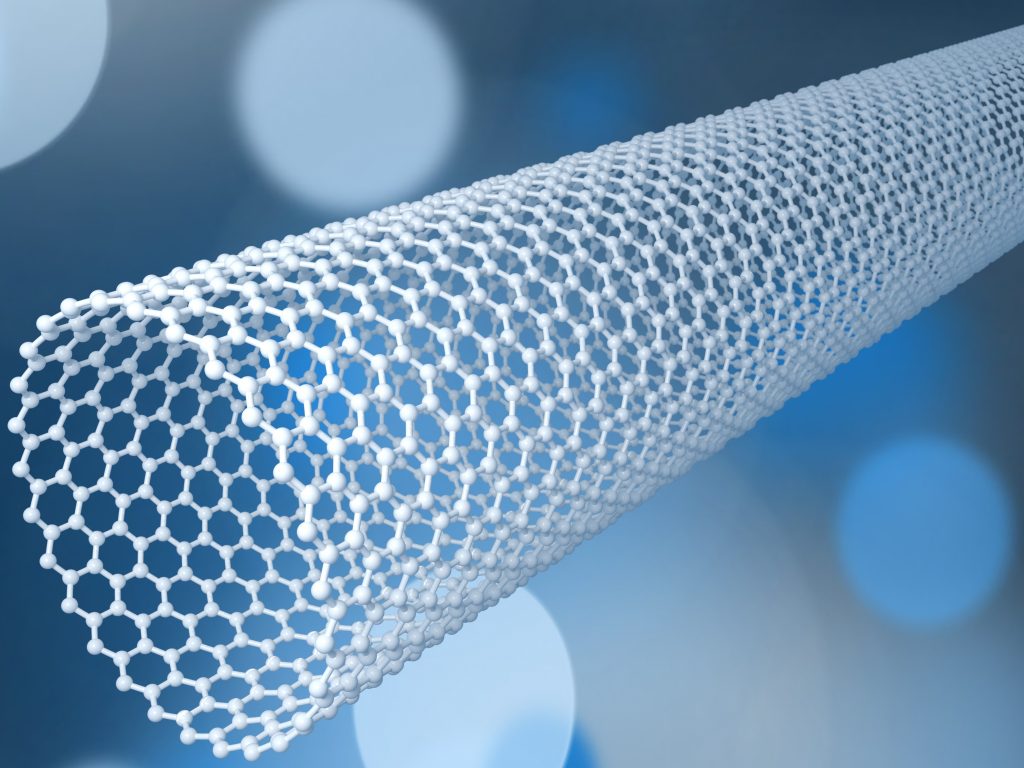
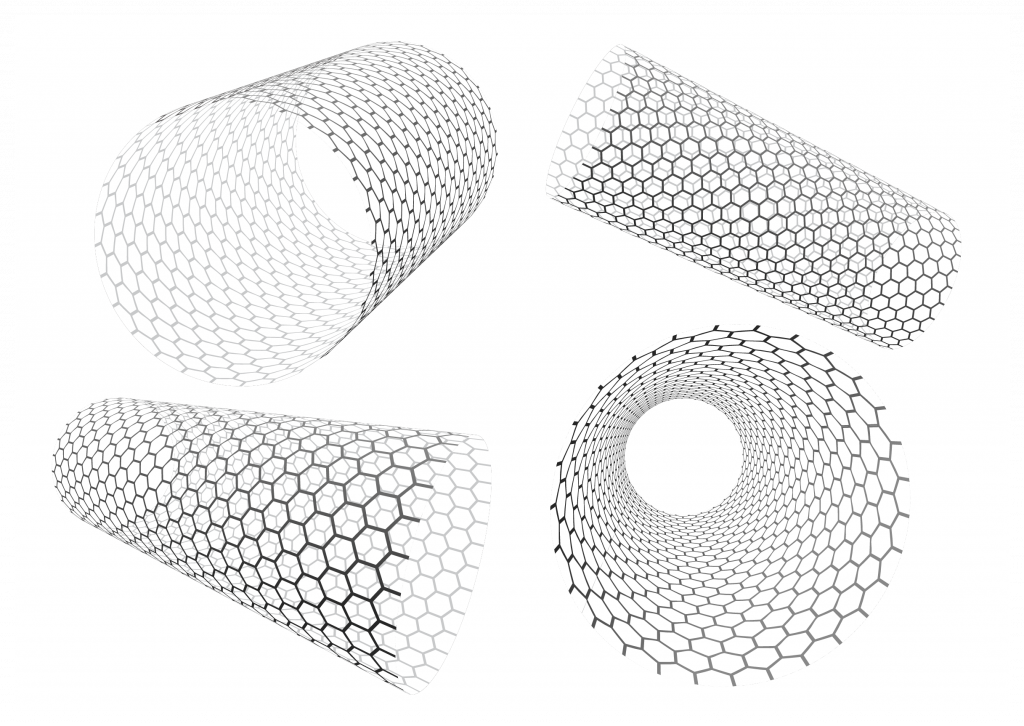
Hiromichi Kataura from the National Institute of Advanced Science and Technology in Japan is well known in the scientific community for his research on physics and applications of carbon nanotubes. Recently him and his team are using carbon nanotubes as small bio probes to image physiological and biochemical activity in-vivo.
Specifically, the researchers are looking at brown adipose tissue (BAT). BAT plays an important role in the regulation of body temperature and when stimulated, anti-obesity and diabetic effects are increased. A deep understanding of the mechanisms in BAT is important for the development of drugs to fight metabolic syndrome.
The researchers describe that the current standard method for observing BAT is positron emission tomography (PET) or histological investigation (ex-vivo). While PET is useful it does not always reflect the metabolic activity of the fat tissue well, so one of Kataura’s goals is to provide new observation methods that correctly correlate to metabolism and allow for in-vivo observations.
The team prepares carbon nanotubes emitting fluorescence light between 1000-1400 nm where light can penetrate deeply in tissue without absorption or scattering by biomolecules. This range also has low tissue autofluorescence. The nanotubes are can be highly adapted to be specific to the BAT tissue. The team shows that the fluorescence signal can be successfully applied to observe the activity in BAT tissue.
The group of Markita Landry at UC Berkely is researching methods to measure and understand the mechanisms of life on the nanoscale. Her group uses Carbon Nanotubes as a fluorescent probe on the nm length scale. Nanotubes can be built to measure different molecules in living systems, but they can also be precisely engineered to emit at certain wavelength by changing their diameter and chirality.
The group published research using nanotube species emitting light at different wavelengths that each target different molecules, multiplexing the collection of information of several biochemical processes. The nanotubes are tuned to emit light in the SWIR/NIR-II range where low absorption and scattering in tissue give the highest spatial accuracy of light emission.
Radiation therapy is one standard method for treating certain types of cancerous tumors. The challenge in all radiation therapies is always to precisely localize the diseased tissue and deliver a lethal radiation dose at exactly that location without damaging surrounding healthy tissues. Brian Pogues group from Dartmouth in Vermont has pioneered the use of gated ICCD cameras to detect Cherenkov light that gets produced by ionizing radiation in matter. Measuring the Cherenkov emission allows this group to measure radiation deposited at certain locations within a human body.
This technology is currently commercialized by a company spun off from Prof. Pogues group. While Cherenkov ligh is mostly emitted in the blue to visible region, SWIR light gives much higher accuracy about the position of radiation in tissue due to the low scattering and absorption by tissue. The researchers are now reporting on using fluorescent quantum dots that are distributed in a tissue sample and designed to absorb the Cherenkov radiation and emit SWIR radiation. The group is now working on applying this technique in radiation therapy as well as imaging molecular processes with targeted nanoscale probes.
Advanced Back-Illuminated CMOS Provides an Alternative to EMCCDs for Dynamic, Faint Astronomy
Overview
Ground-based optical astronomy investigates various objects in space, from galaxies to exoplanets, via visible light. Some of these objects are dynamic and move at high speed through the sky. Traditionally, observation of these dynamic objects and events has been limited to EMCCD cameras due to their fast frame rates and high sensitivity. However, EMCCD cameras are limited by excess noise factor when the signal is greater than a few photons.
The most recent advancements in CMOS imaging technology deliver low read noise and high quantum efficiency within the visible range, increasing their detection capability for ground-based optical astronomy. CMOS cameras, like EMCCDs, also have fast frame rates but are not limited by excess noise factor. Therefore, state-of-the-art CMOS cameras are now the ideal choice for observing dynamic events in space.
Introduction
Ground-based optical astronomy is essential for many astronomical investigations. Most objects in space can be observed via visible light (380-700 nm), to study, for example, supernovae remnants or how stars develop [1]. Some objects and events move in space at high speeds, such as near-Earth objects, requiring a fast camera to capture any changes [2].
One of the limitations of ground-based astronomy is image deformation caused by atmospheric turbulence. Techniques such as adaptive optics and lucky imaging have been developed to counteract the effect of the atmosphere. Lucky imaging is a technique which acquires multiple images very quickly so that turbulence motion is “frozen.” Sharp images can then be collated during post-processing to improve the overall resolution of the image.
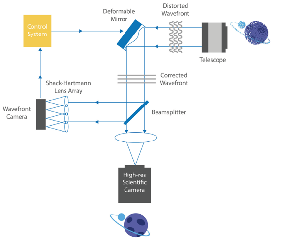
Adaptive optics, another technique, uses wavefront sensing to counteract the effects of atmospheric turbulence. A traditional camera can be transformed into a wavefront sensor by the addition of lenslets. These lenslets can either be located outside of the camera or incorporated into the camera so that they are close to the sensor. The lenslets measure distortions in the wavefront, allowing software to feed corrections back to the telescope to counteract atmospheric distortions. Figure 1 shows a schematic of how an adaptive optics system operates.
Figure 1: Schematic of an adaptive optics system in which a distorted wavefront is measured by a wavefront camera, which feeds the level of distortion into a control system. This control system counteracts the distortion via a deformable mirror which corrects the wavefront to produce a diffraction limited image.
Cameras employing wavefront sensors must have sufficient frame rate to react to the rapidly changing atmosphere, especially when it is unstable. These cameras also require low read noise alongside high sensitivity so that faint reference stars can be used for atmospheric correction. It is not always guaranteed that a bright reference star is located near the scientific object of interest, in which case a faint reference star within close proximity must be used. Therefore, wavefront cameras with higher sensitivity and lower noise are advantageous to capture these fainter reference stars [3].
Although the majority of visible ground-based astronomy utilizes silicon-based CCDs, these sensors are limited when it comes to high-speed astronomy observations. Standard CCD detectorshave relatively high read noise and read out at a slow rate, preventing fainter, dynamic objects from being investigated.
Electron multiplying CCDs (EMCCDs), are a variant of silicon-based CCDs that are able to overcome these limitations through the use of an extended serial register called the electron multiplier register (EM register), on the sensor [4,5]. The EM register uses electron multiplication to elevate electron signal greatly above the read noise floor. This allows for higher sensitivity during low-light acquisition.
When dynamic objects are observed they require faster acquisition in order to capture any changes, however this results in a lower exposure time and therefore minimal photon detection. By using an EM register, EMCCDs are able to amplify any detected photoelectrons before they are read out, making the read noise effectively negligible and allowing for the observation of dynamic, faint objects.
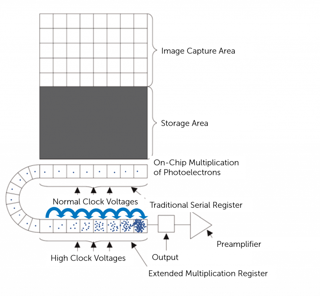
In this EM register, photoelectrons are accelerated via an increased voltage along each stage of the register, with secondary electrons generated via the impact-ionization process (Figure 2). The quantity of secondary electrons can be controlled by altering the clock voltages within the EM register. As this amplification of electrons elevates the signal far above read noise, the read noise can be very high at the point of measurement. This means that the readout process can be driven at a much faster rate than on a regular CCD, achieving higher frame rates.
EMCCD sensors also have frame-transfer architecture in which the sensor is divided into an imaging capture area which captures any incident photons, and the storage area onto which any detected photons are rapidly transferred after acquisition (Figure 2). While the storage area is being read out by the system electronics, the image array can be exposed to light again allowing for continuous operation at high frame rates. This allows EMCCDs to operate at a much faster rate than ‘Full Frame’ CCDs which require a mechanical shutter to close during readout.
Figure 2: Schematic showing the architecture of an EMCCD sensor, with an image capture area and storage area for short frame times and an EM register with on-chip multiplication.
The combination of both negligible read noise and fast readout makes an EMCCD camera a good option for imaging faint, high-speed objects. However, while EMCCDs are an improvement on CCD technology for dynamic observations, they come with their own limitations.
EMCCD Limitations
EMCCDs are ideal for amplifying single-photon signal due to the EM register; however, this advantage breaks down when the signal is greater than a few photons.
Although EMCCDs are able to amplify the signal above the read noise, they are limited by the excess noise factor. When photoelectrons enter the EM register there is a small chance that a photoelectron will be multiplied at each step. As an EM register is comprised of numerous multiplication steps, the number of photoelectrons exponentially increases. This process is stochastic in nature, meaning that small variations in number of photoelectrons multiplied in each step will result in a wide spread of multiplied photoelectrons at the end of the EM register. This spread is described as the excess noise factor, and for any signal above a single photoelectron, the larger the signal that enters the EM register, the larger the excess noise. Therefore, even with low read noise, multiplication can contribute more total noise rather than less at typical signal levels [6,7].
EMCCDs are also limited by EM gain decay, whereby with use, the ability of the EM register to multiply signals diminishes. Although not fully understood, it is thought that charge builds up in the silicon sensor reducing the effect of the EM gain. The EM gain will decay at a faster rate both if a high EM gain is used and if there is a high signal intensity. This means that the EM gain will not remain consistent over long periods of time, limiting quantitative analysis. This reduces the lifespan of an EMCCD, requiring regular calibration and limitation of the EM gain to preserve camera longevity [6].
To find out more about EMCCD sensor technology, please refer to EMCCDs: The Basics.
CMOS for High-Speed Observation
Complementary metal-oxide-semiconductor, (CMOS), sensors are also silicon-based sensors that are able to capture photons within the visible range. Although CMOS sensors have frame times shorter than EMCCDs despite higher pixel counts, and are therefore able to more rapidly acquire data, the traditional front-illuminated sensors were not considered for high-speed astronomical observation due to high read noise and low quantum efficiency.
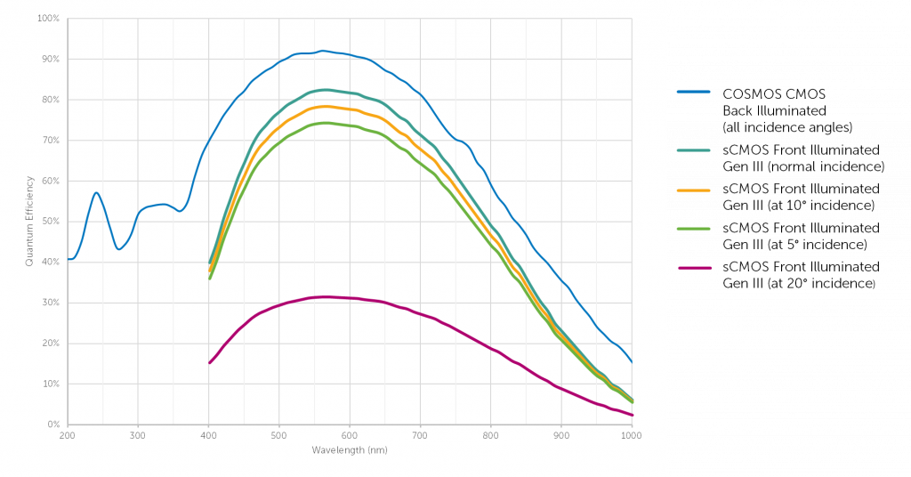
Advancements in CMOS technology have improved the QE and lowered the read noise to match that of a typical EMCCD, without the presence of the excess noise factor. For example, the Teledyne Princeton Instruments COSMOS™ camera offers 0.7 e- read noise due to advanced electronics, with back-illuminated technology providing a peak QE of >90%, as shown in Figure 3.
Front-illuminated CMOS technology illuminates the sensor with incident light from the front, meaning that the miniaturized electronics on each sensor interact with any incoming light first. This reduces the area of the pixel which is sensitive to light. To correct for this, front-illuminated CMOS sensors use microlenses to improve the light-collection efficiency of each pixel, however these microlenses limit the sensor’s peak quantum efficiency, with the quantum efficiency reducing with the incidence angle of incoming light (see Figure 3).
In comparison, back-illuminated CMOS sensors illuminate the sensor from behind, meaning that the incident light interacts with the light-sensitive silicon first. This allows the entire pixel to be light-sensitive and removes the need for microlenses. This change in illumination technology allows for an increase in peak quantum efficiency [8].
Figure 3: Quantum efficiency (QE) of the COSMOS with respect to wavelength, showing 90% peak quantum efficiency, and a typical front illuminated sCMOS Gen III sensor at normal incidence, 10° incidence, 5° incidence and 20° incidence showing how QE drastically decreases in front illuminated with angle of incidence.
Not only does advanced CMOS technology, such as that of the COSMOS camera, match the essential parameters required from EMCCDs when detecting high-speed objects, it does not suffer the same sensitivity limitations of the EMCCD with regards to excess noise factor. CMOS sensors don’t have an EM register, meaning that they do not suffer from excess noise due to the stochastic nature of the multiplication steps. Removing this limitation of EMCCDs allows low-noise CMOS sensors to far exceed EMCCD sensitivity when greater than a few photons are detected. Minimizing read noise is still of the utmost importance, but the 0.7 e- read noise of the COSMOS allows low-light signal to be detected with a high signal-to-noise ratio.
Due to the architecture of CMOS sensors, data can be processed much faster than both EMCCDs and CCDs. CMOS sensors have a miniaturized capacitor and amplifier on each individual pixel, allowing the CMOS sensor to work in parallel, with each converted photoelectron being immediately converted into a voltage while still on the pixel.
CMOS sensors also have an analogue-to-digital-converter (ADC) for each column, rather than a single ADC as with EMCCD sensors. ADCs convert the voltage of electrons into a digital signal which is used to display data. Having an ADC per column means that each ADC has less data to process, therefore the whole sensor is able to process all of the acquired data at a much faster rate. Figure 4 shows a typical schematic of CMOS readout architecture in comparison to that of an EMCCD. This allows CMOS detectors to run at very high frame rates – ideal for dynamic imaging.
Figure 4: Sensor readout architecture of a typical EMCCD and a typical CMOS. The individual electronics on each pixel, and the ADC for each column greatly increases the speed at which acquired data can be processed.
High-speed, ground-based space science applications often require a large field of view in order to sample large areas of the sky. For example, space debris, in particular low-Earth orbit debris, moves quickly across a field of view (in the order of seconds). These objects can be tracked either by leap-frog tracking, in which the object moves across the field of view creating an object arc, or by continuous tracking, in which the object is point like and background stars appear as arcs. Both of these tracking methods rely on the telescope accurately moving either with the object (as with continuous tracking) or predicting the position of the object once it passes the field of view (as with leap-frog tracking) [9].
A camera with a larger field of view can be advantageous for both methods. For example, leapfrog tracking a larger camera FOV results in the object taking longer to traverse across the sensor. This means that fewer telescope movements will be required for imaging the full object trajectory, increasing the accuracy of tracking.
For continuous tracking, a larger camera FOV will result in more background stars for reference, aiding in predictions of object parameters. The COSMOS is one of the largest format CMOS sensors, with sensor sizes of 6k x 6k and above (see Figure 5). In combination with lower read noise and high QE, the COSMOS allows for precise tracking of fainter, and smaller, objects such as low Earth orbital space debris [9].
Figure 5: Graphical representation of the physical size of the COSMOS-42M (6496 x 6496) sensor verses a typical tracking sensor. *Typical sensor based on a 9-micron pixel, 4096 x 4096 CCD sensor.
Summary
Ground-based, high-speed astronomical observations require cameras with high frame rates, fast read-out, and low read noise. Although EMCCDs are traditionally used, they are severely limited when detecting a signal greater than single-photon due to the excess noise generated within the multiplication step.
Previously, CMOS detectors were disregarded for high-speed observations. Although they had fast frame rates and low frame times, they had considerably higher read noise and lower QE than EMCCDs. Advancements in CMOS technology have now allowed for back-illuminated CMOS detectors, such as the COSMOS camera, to provide equivalent read noise and QE to EMCCDs without the sensitivity limitation. The COSMOS incorporates a large format sensor which allows more of the sky to be sampled, something which is advantageous in high-speed applications such as space debris tracking.
[4] S. M. Tulloch, V. S. Dhillon, On the use of electron-multiplying CCDs for astronomical spectroscopy, Monthly Notices of the Royal Astronomical Society, 441, 1, 2011
[5] D. Ives, Electron multiplication CCDs for astronomical applications, Nuclear Instruments and Methods in Physics Research Section A: Accelerators, Spectrometers, Detectors and Associated Equipment, 604, 1-2, 2009
[9] Hampf D., et al., Ground-based optical position measurements of space debris in low earth orbits, Deutsche Luft- und Raumfahrtkongress 2013, 10.09.2013 – 12.09.2013, Stuttgart, 2013
Further Reading
Advanced CMOS for Astronomy
Find out more about how the advancements in CMOS technology can now not only match that of CCD and EMCCD for astronomy, but also overcome some of the common limitations.