Prof. Jana Zaumseil
Heidelberg University,Germany
Background
The group of Prof. Jana Zaumseil at Heidelberg University in Germany investigates novel semiconducting materials with focus on charge transport and application in optoelectronic devices. One research focus of the group is to build and investigate devices based on single-walled carbon nanotubes (SWCNT), one-dimensional structures that can be conceptualized as rolled-up sheets of graphene. In contrast to graphene, nanotubes can be metallic or semiconducting depending on their roll-up vector. By polymer-sorting, the different geometries can be selected. The 1D nature of the nanotubes leads to exceptionally strong bound states between electrons and holes that produce room-temperature stable excitons featuring narrow emission in the NIR. Using chemical functionalization, luminescent quantum defects can be introduced into nanotubes to tune the emission into wavelength regions relevant for telecom application or generate single-photon emission at room-temperature.
This makes nanotubes a promising material for novel optoelectronic devices such as ultrafast transistors, on chip photodetectors or potentially lasers. The group implements new device designs and proves their concept of operation. Jan Lüttgens, a doctoral student and scientist in the lab says that “one interesting aspect of my work is that we can make real devices ourselves to prove their principle of operation and test these concepts in the lab.”
One such concept, that is implemented in his experiments, is realized by embedding nanotubes in photonic structures, such as Fabry-Pérot cavities or plasmonic crystals which enhance their coupling to the electromagnetic field. Under the right conditions the device can be brought into the strong light-matter coupling regime which creates new hybrid states called exciton-polaritons. The strong coupling regime requires an optimized device design and can be tuned by contacting the nanotubes electrically to suppress excitations in the material or to pump the new hybrid-states electrically or even create charged-light-matter particles. Strong coupling between nanotubes and a cavity can also be used to fabricate photodiodes that can absorb light far-beyond the intrinsic nanotube band gap.
Challenge
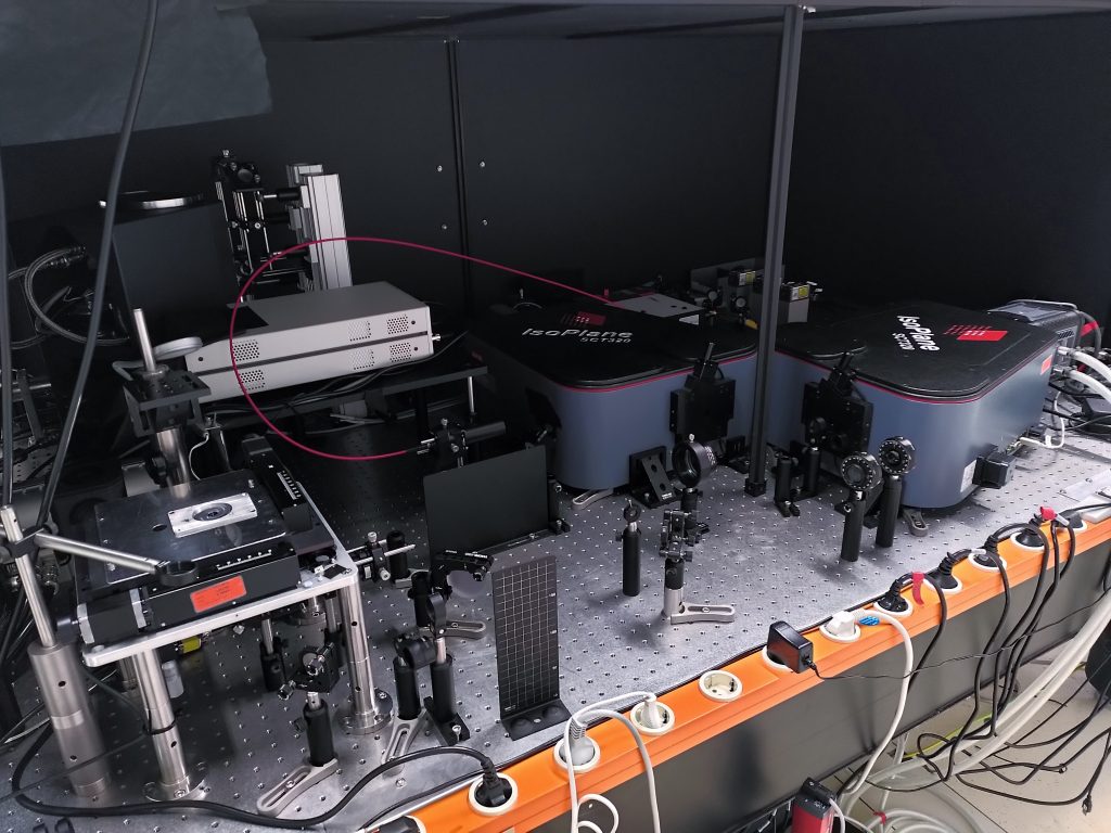
An indicator for the presence of strong coupling between the nanotube states and the electromagnetic field is a characteristic mode splitting at the exciton energy in reflectivity and emission. For efficient observation of the mode structure the lab uses a technique called Fourier imaging spectroscopy. By inserting an additional lens into the beam path the cavity mode structure can be resolved in momentum and energy simultaneously by one-shot measurements. Compared to scanning based techniques it increases the measurement efficiency by reducing the acquisition time using a two-dimensional detector. Furthermore, tomography of the mode structure can be achieved by simply shifting the Fourier image relative to the detector. For NIR (or SWIR) emitters, this requires cameras which are sensitive in the wavelength range between 1-1.7μm.
However, NIR emitters usually suffer from low photoluminesence quantum yields and low dimensional materials additionally exhibit saturation effects at comparably low excitation powers. Working in the linear regime, therefore, requires low thermal noise detectors, to enable long integration times.
“In the NIR, the emission efficiency of materials drops drastically, so it is good to have low thermal noise.”
Solution
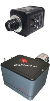
The Fourier Imaging setup of the Zaumseil group uses a NIRvana 640 camera and Isoplane spectrograph to enhance the capability for detection of the low light emission from nanotube devices and single tube samples. The two-dimensional InGaAs detector of the NIRvana camera with high quantum efficiency in the NIR, enables such experiments. The sensor of the camera is thermoelectrically cooled to -85⁰C to reduce the dark current on the sensor and an integrated cold shield system limits the influence of thermal background radiation on measurements. This makes the NIRvana 640 ideal for measurements of the weak signals that can require several seconds or more of integration time, combined with imaging capabilities of 2D detector array
The Isoplane spectrograph is designed to eliminate astigmatism and minimize optical aberrations that could distort the spectral images in the focal plane. Such a design increases the quality of spectral data across the whole focal plane of the spectrograph, which improves measurements such as Fourier Imaging Spectroscopy that use a large or even the whole sensor area of the camera.