
Background
Scientific cameras are essential for taking images of scientific research to understand the phenomena surrounding us. A key aspect of scientific cameras is that they are quantitative, with each camera measuring the number of photons (light particles) which interact with the detector.
Photons are particles which create the electromagnetic spectrum, from radio waves to gamma rays. Scientific cameras usually focus on the UV-VIS-IR region to quantify visual changes within scientific research.
Each scientific camera has a sensor which detects and counts photons which are emitted in the UV-VIS-IR region. These photons are usually emitted from the sample.
Sensors
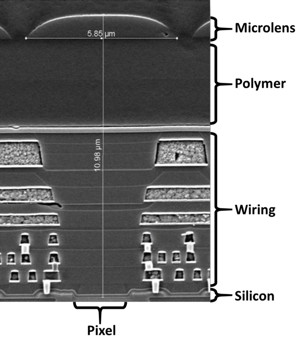
The function of a scientific camera sensor is to count any detected photons, and then convert them into electric signals. This is a multistep process which begins with the detection of photons. Scientific cameras use photodetectors, which convert any photons that hit the photodetector into the equivalent number of electrons. These photodetectors can be made of different material dependent on the wavelengths of the photons that are being detected, however silicon is most common for the visible wavelength range. When photons from a light source hit this layer, they are subsequently converted into electrons. An example of a silicon photodetector can be seen in Figure 1.
Pixels
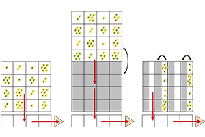
In order to create an image, more than just the number of photons hitting the photodetector needs to be quantified. The location of the photon on the photodetector also needs to be known. This is done by creating a grid of many tiny squares on the photodetector, allowing for both detection and location of pixels. These squares are pixels, and technology has developed to the point where you can fit millions of them onto a sensor. For example, a sensor that is 1 megapixel contains one million pixels. A visualization of this can be seen in Figure 2.
To fit so many pixels onto a sensor, they have been developed to be very small, however the sensor itself can be quite large in comparison. An example of this would be the SOPHIA 4096B camera, which has 15 μm square pixel size (an area of 225 μm2 ) arrange in an array of 4096 x 4096 pixels (16.8 million pixels), resulting in a sensor size of 27.6 x 27.6 mm (area of 761.8 mm2) with a diagonal of 39.0 mm.
A compromise, however, needs to be made with the size of the pixels. Although decreasing the size of the pixel will increase the number that can be placed on a sensor, each individual pixel will not be able to detect as many photons. This introduces a compromise between resolution and sensitivity. Alternatively, if the sensors are too big, or contain too many pixels, much greater computational power is required to process the output information, decreasing image acquisition. This adds additional issues such as large information storage, with researchers requiring very large storage to save multiple experimental images for long periods of time.
Therefore, sensor size, pixel size and pixel number all need to be carefully optimized for each scientific camera design.
Generating An Image
Each pixel within a sensor detects the number of photons that come into contact with it, after being exposed to a light source. This creates a map of photon count and photon location, known as a bitmap. A bitmap is an array of these measurements and is the basis behind all images taken with scientific cameras. The bitmap of an image is also accompanied by the metadata, which contains all image information, such as camera settings, time of image, and any hardware/software settings.
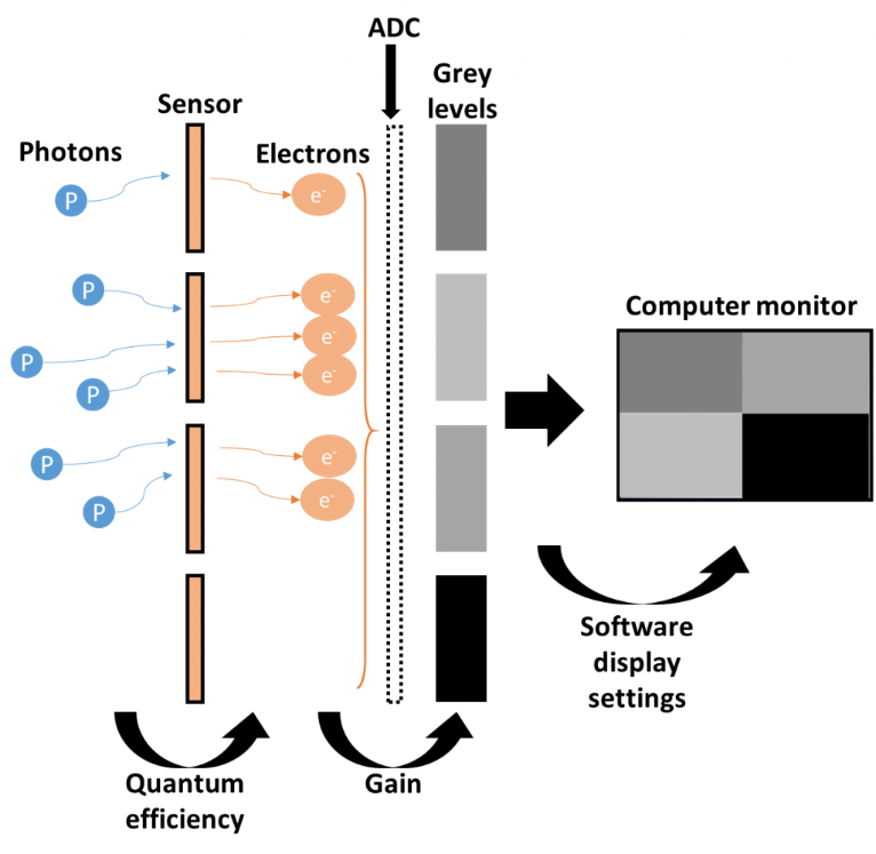
The following are the processes involved in creating an image with a scientific camera, with each step visualized in Figure 3:
- Any photons that hit the photodetector are converted into photoelectrons. The rate of this conversion is called quantum efficiency (QE), with 50% QE referring to 50% of the photons being converted into electrons.
- Generated electrons are stored in a well within each pixel, provided a quantitative count of electrons per pixel. The maximum number of electrons stored within each well controls the dynamic range of the sensor, as described by well depth or bit depth.
- The number of electrons per well are converted from a voltage into a digital signal (gray levels) with an analogue to digital converter (ADC). The rate of this conversion is described as gain, where a gain of 1.5 will convert 10 electrons into 15 gray levels. The color generated from 0 electrons is known as the offset.
- The gray levels (corresponding to the digital signals) are arbitrary grayscale (monochrome) colors. These gray levels are dependent on the dynamic range of the sensor and the number of electrons in the well. For example, if a sensor is only capable of displaying 100 gray levels, then 100 gray levels would be bright white (i.e. saturated). However, if the sensor if capable of displaying 10,000 gray levels, then 100 gray levels would be very dark. This is assuming that no scaling has been applied.
- A map of these gray levels is displayed on the computer monitor. The image generated depends on the software settings, such as brightness, contrast, etc. that are included in the metadata
Gray levels are dependent on the number of electrons stored within the wells of a sensor pixel. They are also related to offset and gain. Offset is the gray level baseline, with the value corresponding to no stored electrons. Gain is the rate of conversion of electrons to gray levels, with 40 electrons converted to 72 electrons with a 1.8x gain, or to 120 electrons with a 3x gain. In addition to gain and offset, the imaging software display settings also determine how the converted gray levels and the image displayed on the computer monitor correspond to each other. These display settings affect the visualization of the gray levels, as they are arbitrary, and are reliant on the dynamic range of other values across the sensor. These predominant stages of imaging are consistent across all modern scientific camera technologies, however there are variations between sensor type and camera models.
Types Of Camera Sensor
Sensors are the main component of the camera and are continually being developed and optimized. Researchers are constantly looking for better sensors to improve imaging, providing better resolution, sensitivity, field of view and speed. There are many different camera sensor technologies, which vary in properties such as high sensitivity over different wavelength ranges. These sensors include charge-coupled devices (CCD), electron-multiplied CCDs (EMCCD), intensified CCDs (ICCD), indium gallium arsenide semiconductors (InGaAs), and complementary metal-oxide-semiconductors (CMOS), all of which are discussed in separate documents.
Summary
A scientific camera is essential for any imaging system. These cameras are designed to quantitatively measure how many photons hit the camera sensor and in which location. These photons generate photoelectrons, which are stored in wells within the sensor pixels before being converted into a digital signal. This digital signal is represented by gray levels and displayed as an image on a computer monitor This process is optimized at every stage in order to create the best possible image dependent on light signal received.
Further Information
CCD Sensors
CCD sensors are silicon based semiconductors which capture photons and covert them into photoelectrons. This is converted into a digital signal and read out by the camera.
EMCCD Sensors
Electron multiplying CCD (EMCCD) sensors are a variant of CCDs which capture a low number of photons and convert them into a high signal.
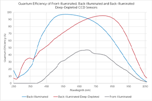
Quantum Efficiency
Quantum efficiency is the percentage of photons that an imaging device can convert into electrons. It is dependent on sensor material and wavelength of light being detected.